当前时间:
![]()

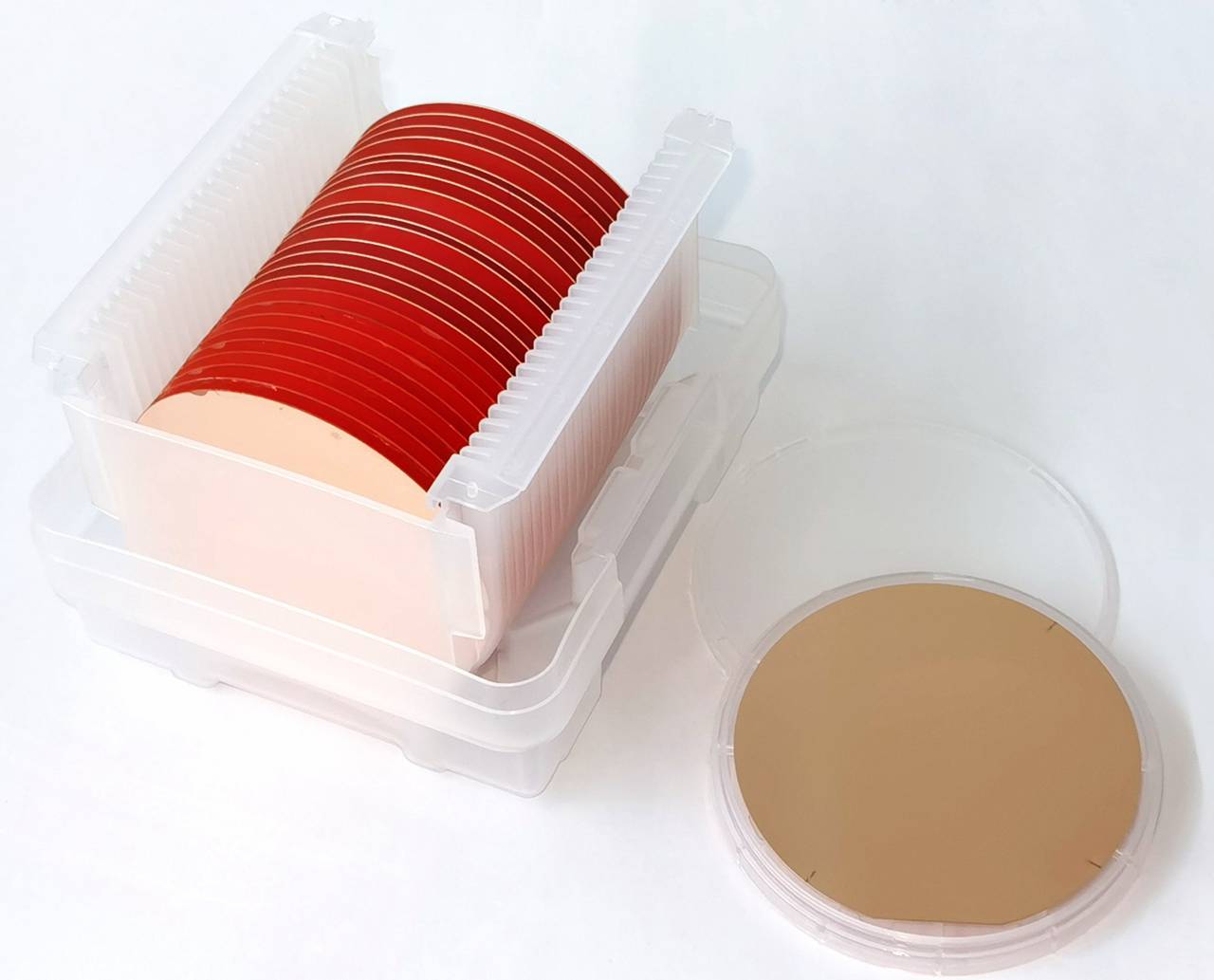
通过"磁控溅射+固相外延重结晶"的技术制备铜单晶晶圆,进而在铜单晶衬底上外延生长得到单晶石墨烯晶圆。利用界面结合力与热应力工程消除了石墨烯的褶皱与台阶束,使其粗糙度(RMS)降低至1nm以下。相较于普通CVD石墨烯薄膜,单晶石墨烯晶圆具有更高的平整度,媲美机械剥离石墨烯的超强机械性能以及超高的均一性,是石墨烯应用于高性能电子及光电子器件集成的理想材料。
The single crystal copper wafer was prepared by the technology of "magnetron sputtering + solid phase epitaxial recrystallization", and then the single crystal graphene wafer was produced by epitaxial growth on the single crystal copper substrate. We eliminate the wrinkles and step bundles of graphene via interface bonding force and thermal stress engineering, which decrease its roughness (RMS) to less than 1nm. Compared with ordinary CVD graphene films, single crystal graphene wafers have higher flatness, better mechanical properties and ultra-high uniformity. Graphene is used in high-performance electronic and optoelectronic devices. Single-crystal graphene wafers are ideal materials for the integration of high performance electronic and op

官方微信


